


Company
Founded in Cambridge, United Kingdom, in August 2026, to develop high speed data converters and transceivers. The name is a combination of Boudica, baud and IC, pronounced bɔːdɪ.kə, ボーディカ.
Vision
We want to digitise all data transmission, in line with existing industry trends. RF baseband processing has been digital for almost three decades, and we helped make coherent optical transceivers possible. SerDes is now undergoing the same transition. We will focus our efforts on all applications that could benefit from this approach. The task is not easy, though. Moving signal processing to DSP requires replacing analogue front-ends with application-specific, high-speed data converters. Such converters typically connect directly to high-speed or RF I/O, require a significant amount of digital calibration and correction, push the limits of semiconductor and packaging technology, and generally form large and complex systems on their own. Their performance, reliability, and power consumption ultimately define the characteristics of the whole transceiver. Therefore, designing these data converters, their associated functions, and complete transceivers based on them is a key capability for making this vision a reality.
Team
We have two decades of experience designing and validating high-speed converters, building design teams from scratch, and occasionally helping struggling converter development programmes. This experience came at the cost of product delays and additional test chips, including some of our own - expensive lessons given the cost of missed product windows and tape-outs.
As Baudica Limited has just been formed, the only official member of the team is the founder, Andrzej Radecki. The team will expand over time, initially drawing on highly experienced teams we have built previously.
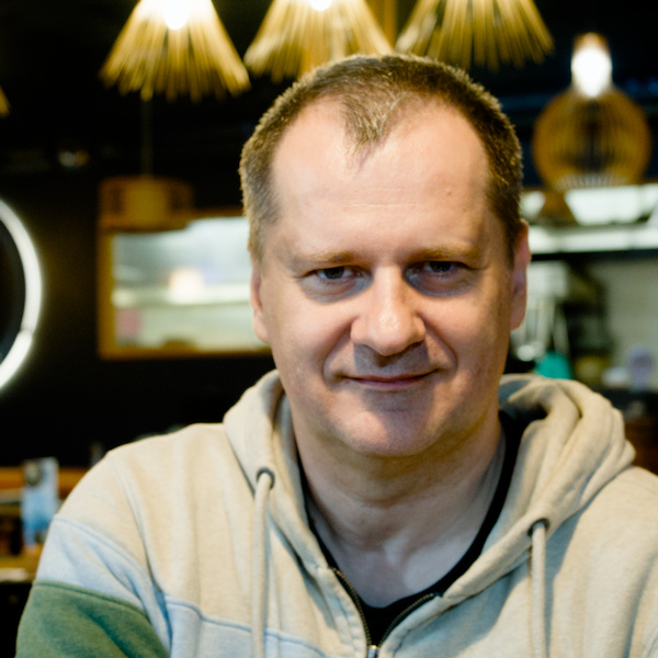
Andrzej Radecki
Products
We are targeting a range of high-speed data converters and transceivers based on them. Potential applications include wireline, optical, RF/satellite, and SerDes systems, which are in high demand in multiple market segments: communication, data-centres, computing, AI. We will also offer smaller parts of the design, such as advanced PLLs, A-to-D converters and other building blocks that can be made reusable at early stage with little additional effort.
Initial development focuses on a specific application and uses a CMOS technology we selected. This approach reduces development time and makes the best use of our available resources. Portability to other applications and technologies is one of our key design goals and it is possible thanks to our experience with multiple applications and CMOS nodes down to 2nm. Please contact us if you would like to sponsor the development of a specific data converter or transceiver suitable for your product.
We are also considering taping out our first device in chiplet form, which could be useful in certain applications, such as metrology. This is not confirmed yet, as it would lengthen the development time. Please contact us if you are interested in evaluating such a design.
Investment Strategy
This is a field with a high barrier to entry, which poses challenges related to development costs. The key barrier - expertise - has already been addressed and the team is partially assembled and actively working on the design. Several technology and CAD vendors are supporting us in this effort. Please contact us if you think your technology or tools would be applicable to this development.
These challenges affect our competitors too. In general, the competitive landscape is still sparse. Larger companies are often operating within their existing business models - either design this type of IP for internal use in a specific application, or bundle it with their technology or service offerings. Smaller vendors are often acquired early or are struggling due to limited expertise and resources.
Additional investment would help us scale significantly faster and address more expensive, high-growth applications, such as SerDes or optical transceivers - both currently in very high demand due to AI growth. We can develop even the most challenging transceivers using a wide range of CMOS technologies. Please contact us if you would like to help us grow.